Applications
Thin film measurements for a wide variety of films
Capabilities
Instrument Performance
Automated Mapping
In Situ ALD
Publications
Capabilities
Film Sense Multi-Wavelength ellipsometers excel at measuring the thickness and index of refraction of transparent single films. The upper thickness limit depends on the ellipsometer system (typically 2 – 5 μm), but is also dependent on the substrate and film optical constants. As with any ellipsometer system, a minimum film thickness (typically 10 nm) is required to obtain accurate index of refraction measurements (the new Liquid Cell option can remove this limitation).
Optically absorbing films can also be measured, but the data analysis becomes more complicated as the film optical constants (both n and k values) are required. The Film Sense software contains multiple methods for determining n&k values: 1) multi-sample analysis, 2) combined ellipsometry + transmission measurements, 3) immersion ellipsometry with the new Liquid Cell option, and 4) dispersion models. The upper thickness limit for absorbing films is strongly dependent on the type of material; for metallic films, the upper limit is typically 50 nm.
Multi-Wavelength Ellipsometry can also be used to measure multilayer film stacks (in some cases up to 5 layers), depending on the thicknesses and indices of refraction of the layers. Simulations can be performed in the Film Sense software to determine if a particular sample structure is possible. For some samples, surface roughness and index gradients in the film can also be characterized.
Send Us Your Samples
As thin film measurement applications are so varied and diverse, the best way to determine if a Film Sense Multi-Wavelength Ellipsometer is right for your application is to perform demonstration measurements on your actual samples. Please contact us to discuss your application, and arrange for sample measurements.
Performance
The typical Film Sense ellipsometer thin film measurement Accuracy and Precision for a variety of samples, including a multi‐layer sample, is shown in the table below. For more details on the testing methodology, contact Film Sense and request our “FS‐8 Performance” white paper.
Click the Sample Type in the chart below to view examples:
|
Sample |
Parameter |
Accuracy |
Precision |
|
Thickness |
0.013 nm |
0.00026 nm |
|
|
Thickness Index @ 633 nm |
0.11 nm 0.0005 |
0.00041 nm 7.3E-6 |
|
|
Thickness Index @ 633 nm |
0.60 nm 0.0001 |
0.0038 nm 3.3E-6 |
|
|
Top SiO2 Thickness Si3N4 Thickness Bottom SiO2 Thickness SiO2 Index @ 633 nm |
0.04 nm 0.08 nm 0.10 nm 0.0003 |
0.0023 0.0032 0.0038 4.3E-6 |
|
|
Thickness Index @ 633 nm |
0.002 nm 0.004 |
0.00030 nm 3.3E-4 |
|
|
Thickness Index @ 633 nm k @ 633 nm |
0.042 nm 0.0011 0.0006 |
0.001 nm 1.1E-5 8.3E-6 |
|
|
Thickness Surface Roughness Index @ 633 nm k @ 633 nm |
0.59 nm 0.004 nm 0.0013 0.0001 |
0.0036 nm 0.0011 nm 1.3E-5 1.6E-6 |
|
|
Thickness Surface Roughness Index @ 633 nm |
0.29 nm 0.12 nm 0.0006 |
0.0031 nm 0.0012 nm 1.7E-5 |
|
|
Thickness Oxide Thickness Band Gap |
0.08 nm 0.02 nm 0.0024 eV |
0.0009 nm 0.00054 nm 5.7E-5 |
|
|
Thickness Resistivity |
0.042 nm 1.1 uOhm-cm |
0.00047 nm 0.02 uOhm-cm |
AUTOMATED MAPPING
Thin Film Measurement Examples
Film Sense Automated Mapping Systems are fast, easy to operate, and can characterize thickness uniformity on wafers up to 300 mm in diameter. Click on the buttons below for examples of thin film measurements from Film Sense Automated Mapping Systems.
“The system (FS-XY150) is great and we are having an increase of users using it. I am happy with the system and I direct users to use it when I am training them on our ALD deposition system. It gives great results and the customer support is quick and helpful too.”
– Tony Whipple, Scientist
Minnesota Nano Center
FS-1 Multi-Wavelength Ellipsometer
ALD In Situ Applications
Film Sense Multi-Wavelength Ellipsometers are ideal for Atomic Layer Deposition (ALD) applications.
- The excellent thickness precision can easily resolve the sub-monolayer thickness changes for individual ALD cycles
- The compact design simplifies the mounting and integration with ALD reactors for in situ thin film measurements
- The in situ, real time thickness data provided by the FS-1 can significantly reduce the ALD process development time when exploring new process parameters and precursors. For example, see our latest paper, which used a Film Sense FS-8 in situ ellipsometer to characterize the ScN GPC vs. process conditions: “Ultrahigh purity plasma-enhanced atomic layer deposition and electrical properties of epitaxial scandium nitride“
- If in situ thin film measurements are not possible (ports on the ALD chamber are required to provide access for the optical beam), the FS-1 can still provide accurate ex situ thickness measurements for very thin ALD films, at an affordable price
Film Sense Ellipsometers have been installed for in situ thin film measurements on many different ALD reactors, including custom designs, commercial reactors, and on the applications below.
Testimonials
“These FS-1 ellipsometers are one of the best upgrades to our atomic layer processing reactors, and have now become an integral part of all our experiments on ALD and ALE.”
Dr. Sumit Agarwal – Colorado School of Mines
“The Film Sense FS-1 in situ ellipsometer has greatly facilitated data acquisition and understanding of the thin film deposition processes in our lab. The instrument was relatively easy to incorporate onto a vacuum chamber, and includes a user-friendly manual and tutorial to explain basic operation. With this tool, we are able to collect much more information during a deposition, including measurements between ALD half-cycles that are not feasible with ex situ techniques. These ellipsometers have become an integral part of our laboratory research, and we look forward to continuing to work with Film Sense in the future.”
Rachel Nye, PhD – student in Chemical Engineering
Parsons Research Group, North Carolina State University
“Overall performance, affordability and ease of use has made the FS-1 a workhorse for our ALD process as well as equipment development efforts. The next generation FS-1EX provides a combination of higher beam intensity and wider spectral range improving both precision and accuracy. For metallic thin films such as TiN, Pt and Ru, two additional IR wavelengths enhance the ability to monitor film thickness and resistivity in-situ during growth. This enhanced performance helps us to streamline development efforts by effectively understanding the impact of different process conditions on film quality in real-time.”
Bruce Rayner – Principal Scientist
Atomic Layer Deposition, Kurt J. Lesker Company
Click here to learn more about how Kurt J. Lesker Company is using Film Sense Ellipsometers.
“The Film Sense FS-1 is a powerful and reliable tool for in-situ characterization of ALD films. The real-time dynamic thickness measurements were critical to understanding the growth characteristics of multicomponent oxides, such as lead zirconate-titanate (PZT), which I studied for my dissertation research through the University of Maryland. The in-situ thickness data I collected with the FS-1 allowed me to screen precursors much more quickly than if I had to rely on ex-situ characterization methods. I continuously used the FS-1 for over five years and haven’t experienced any downtime other than during occasional realignments when switching from ex-situ to in-situ measurement modes. The FS-1 would make a valuable addition to any laboratory looking to enhance their nondestructive thin-film thickness measurement capability.”
– Nicholas A Strnad, Ph. D.
“To summarize our nearly 5-year ownership experience of the FS-1 tool, all I can say, it’s most probably by far the highest performance/cost tool I have ever acquired in my independent research career. Besides the tool itself, as an ellipsometry expert, Film Sense has been very responsive to our data analysis/fit inquiries and saved us valuable research time by sharing his expertise. We are looking forward to getting their latest generation system with additional features that we can integrate for good on either of the reactors. Right now, our single FS-1 tool is going back-and-forth between thermal and plasma reactor based on our needs.”
– Necmi Biyikli, Assistant Professor,
Electrical and Computer Engineering, University of Connecticut
Click here to learn more about how University of Connecticut
is using Film Sense Ellipsometers as part of their research..
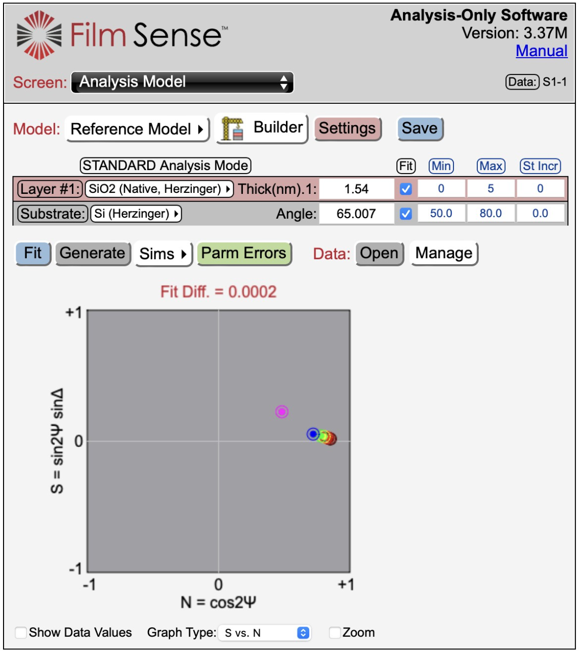
Sample #1: 2nm Native Oxide on Si
A simple one layer model was used to analyze the data from this sample, using book value optical constants for the Si substrate and native oxide film. The fit parameters were the oxide thickness (Layer #1) and the angle of incidence. Note that Si optical constants from Herzinger (https://doi.org/10.1063/1.367101) were used in the model, as they provide an improved fit to the FS-8 data set (especially in the UV), compared to the Jellison Si optical constants (https://doi.org/10.1016/0925-3467(92)90015-F) used with previous Film Sense ellipsometers.
Sample #2: 90 nm Oxide on Si
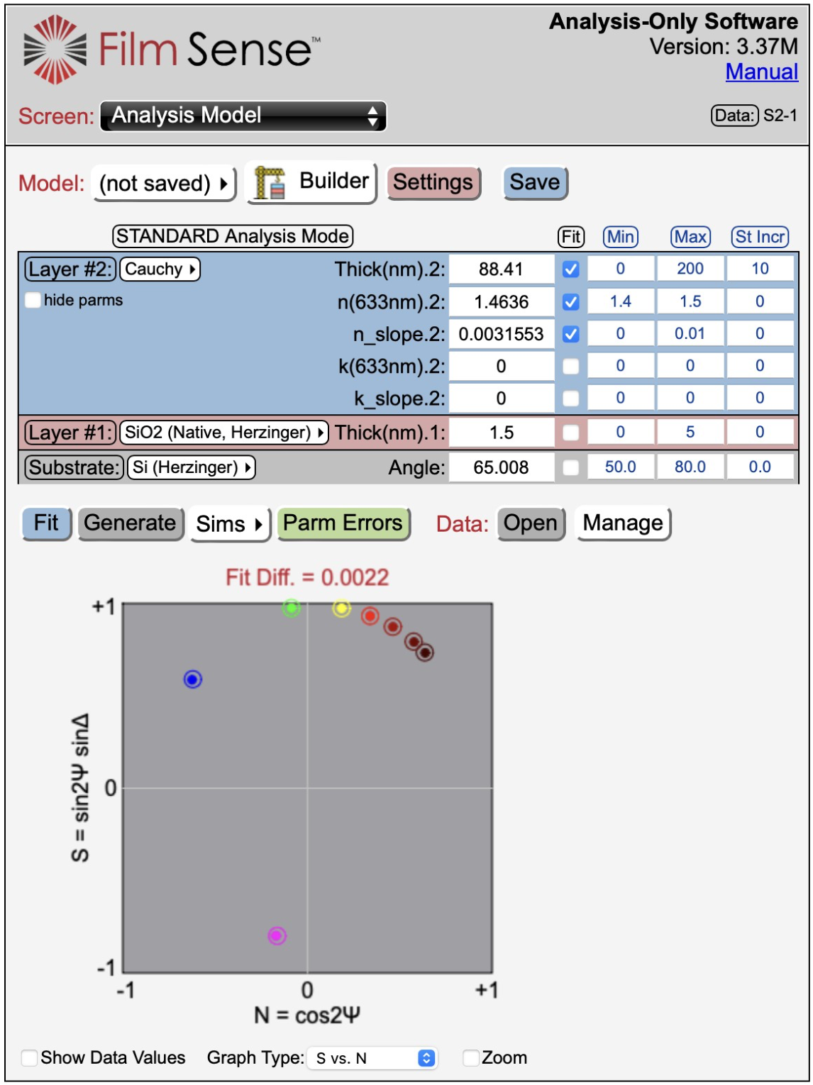
The oxide film on this sample was grown by dry thermal oxidation. In addition to the film thickness, 2 Cauchy terms were fit to determine the index of refraction of the film (the angle of incidence was fixed at its nominal value). A native oxide layer with a fixed thickness of 1.5 nm was also included in the optical model.
Sample #3: 1000 nm Oxide on Si
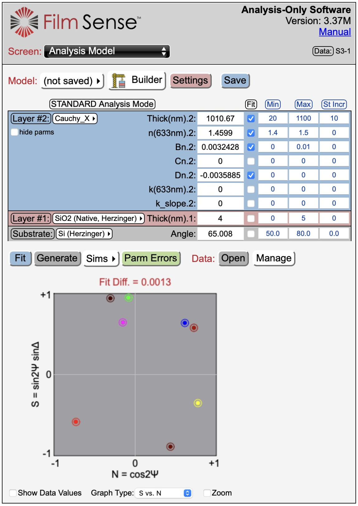
A thick thermal oxide (wet) was grown on this sample. In addition to the film thickness, 3 Cauchy terms were fit to determine the index of refraction of the film (the angle of incidence was fixed at its nominal value). A native oxide layer with a fixed thickness of 4 nm was also included in the optical model.
Sample #4: 100-50-100 nm ONO on Si
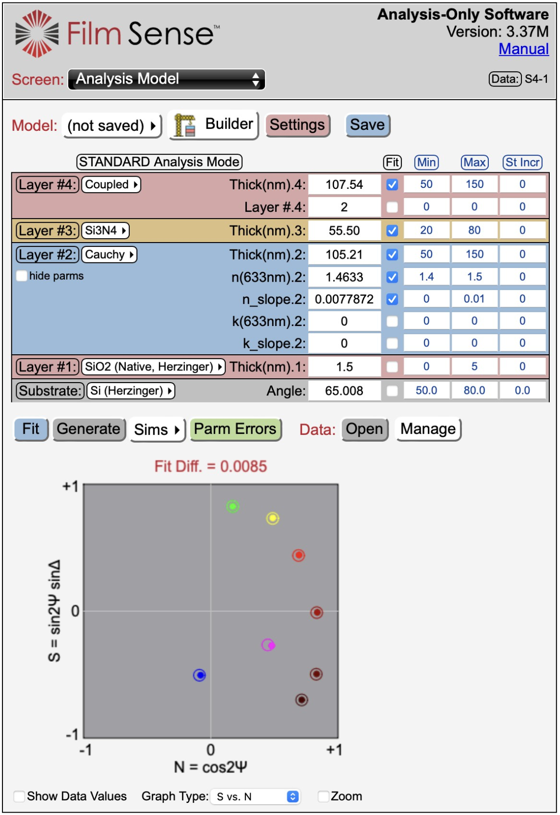
This 3 layer Oxide-Nitride-Oxide structure was deposited by Plasma Enhanced Chemical Vapor Deposition (PECVD). All 3 layer thicknesses were determined by the FS-8. In addition, the SiO2 index of refraction was also fit, assuming that the top and bottom oxide layers had the same index (by using a “Coupled” layer). Book value optical constants were used for the Si3N4 layer.
Sample #5: 6 nm TiO2 on Si
This very thin film was deposited by Plasma Enhanced Atomic Layer Deposition (PEALD). Both the film thickness and index were fit, which is pushing the data analysis limits for films less than 10 nm. However, the UV wavelength (at 370 nm) in the FS-8 data set is helpful in de-correlating the film thickness and index, and excellent matching is still obtained across the 3 systems.

Sample #6: 70 nm Al2O3 on Si
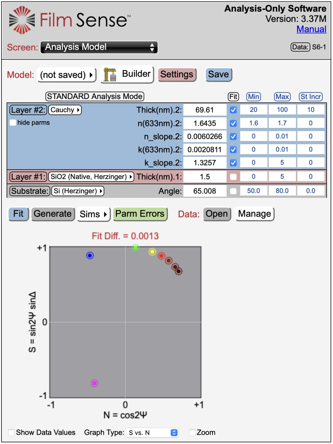
This film was also deposited by Plasma Enhanced Atomic Layer Deposition (PEALD). Adding absorption to the film (by fitting the 2 Cauchy “k” parameters) significantly improved the fit (i.e., the Fit Diff was ≈ 3x lower). The film thickness, index “n”, and absorption “k” were all fit in the analysis, and good agreement was observed in the values determined on the 3 FS-8 systems.
Sample #7: 500 nm SiNx on Si
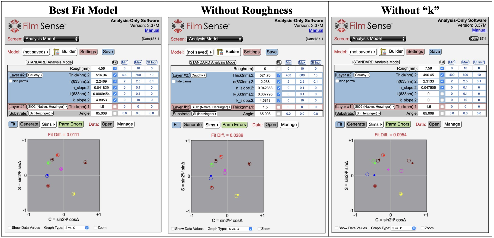
This Si nitride film was deposited by Low Pressure Chemical Vapor Deposition (LPCVD), and the deposition was optimized for low film stress (which requires a Si-rich stoichiometry). Obtaining a good data fit for this sample required a rather complicated optical model, which included both a surface roughness layer, and absorption in the film (i.e., “k” was > 0). 6 fit parameters were uniquely determined in the best fit model.
The model on the left shows the best fit model, which results in a Fit Diff = 0.0111. In the center model, the surface roughness thickness is set to zero, and the Fit Diff increases to 0.0289. The model on the right fixes the “k” parameters at zero, resulting in a ≈ 9x Fit Diff increase to 0.0954. The dramatic improvement in the Fit Diff by adding roughness and “k” as fitting parameters justifies the complexity of the optical model. Note that the Fit Diff could be further reduced by using a more complex dispersion model for the SiN film (Tauc-Lorentz), which will be used for Sample #9 in this study.
Even with the complex optical model, good matching and precision is observed in all the fit parameters. While FS-8 can not always determine the film thickness, surface roughness, index of refraction, and absorption (“t”, “n”, and “k”), it was possible for this particular sample.
Sample #8: 300 nm Ta2O5 on Glass
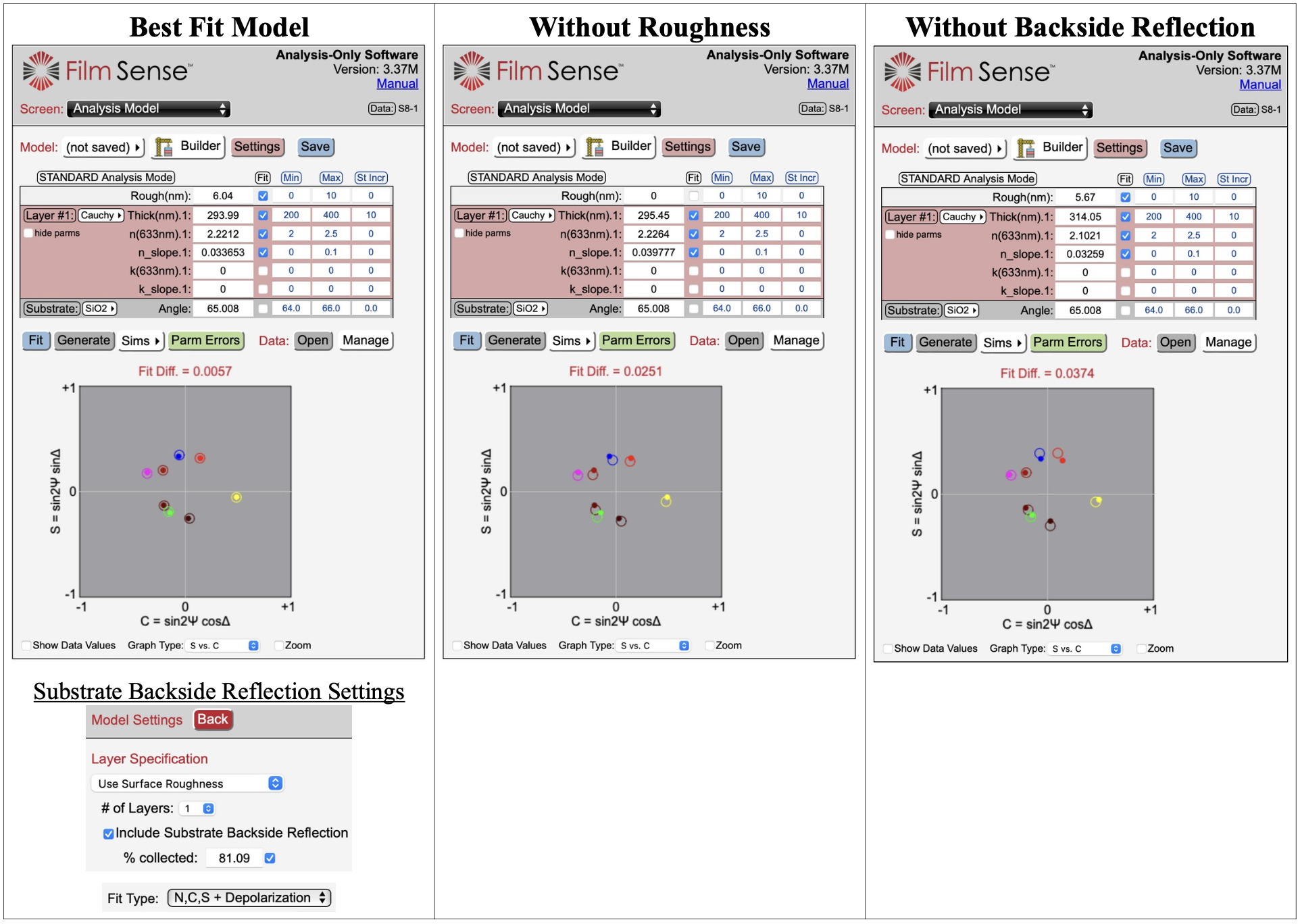
A transparent Cauchy layer was used to determine the index of the Ta2O5 film, and book value optical constants were used for the fused silica substrate. For films deposited on transparent substrates, the reflection from the polished backside of the substrate can affect the measured ellipsometric data. The Film Sense software can account for the back side reflection by checking the corresponding box in the “Model Settings” screen. Since this substrate was 1.6 mm thick, only a portion of the backside reflection (≈ 80%) was collected, which was determined by fitting for this parameter, and including the ellipsometric “Depolarization” data in the analysis. If surface roughness and backside reflection are not included in the model, the Fit Diff is 4 – 6x higher compared to the Best Fit Model (shown below left).
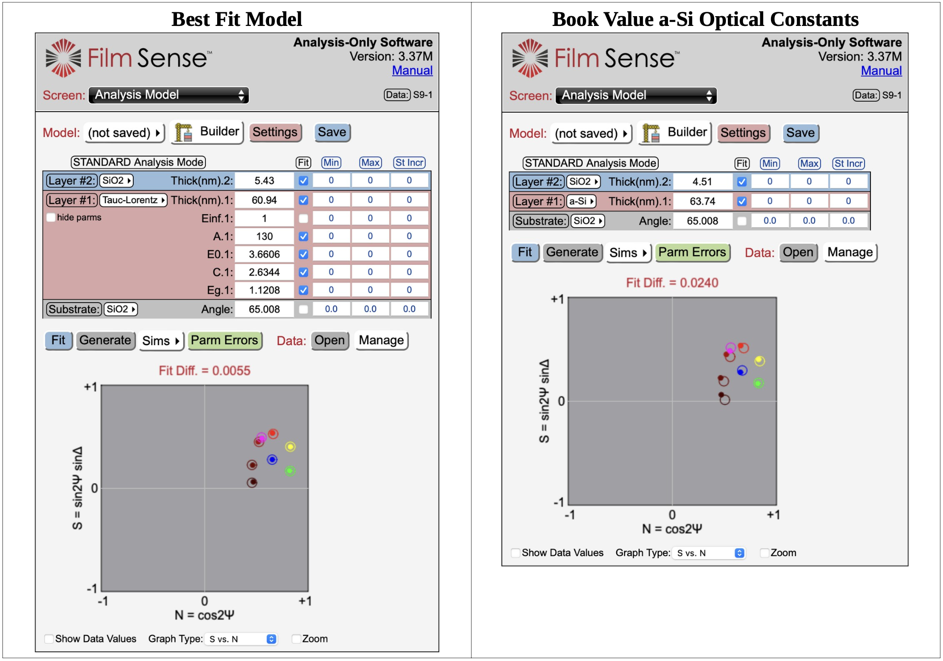
Sample #9: 60 nm a-Si on Glass
Amorphous silicon (a-Si) is an absorbing material, and its optical properties are strongly dependent on the deposition conditions. Using book value a-Si optical constants, a qualitative fit could be obtained, as shown in the model below right. Book value optical constants were also used for the fused silica substrate (which also included the backside reflection), and the oxidized surface layer on the film.
A much better fit was obtained by fitting for the a-Si optical constants, using a Tauc-Lorentz (T-L) dispersion layer, as shown in the model below left. The T-L dispersion equation (G.E. Jellison Jr. and F.A. Modine, Appl. Phys. Lett. 69 (3), p. 371, 1996) works well for many amorphous semiconductor materials, and the parameter definitions are: Einf (ε1 at infinity), A (oscillator amplitude), E0 (oscillator energy), C (oscillator broadening), and Eg (band gap). It is typically assumed that spectroscopic data is required to determine the T-L oscillator parameters, but the results below demonstrate that good precision and accuracy can also be obtained from the FS-8 multi-wavelength ellipsometric data set.
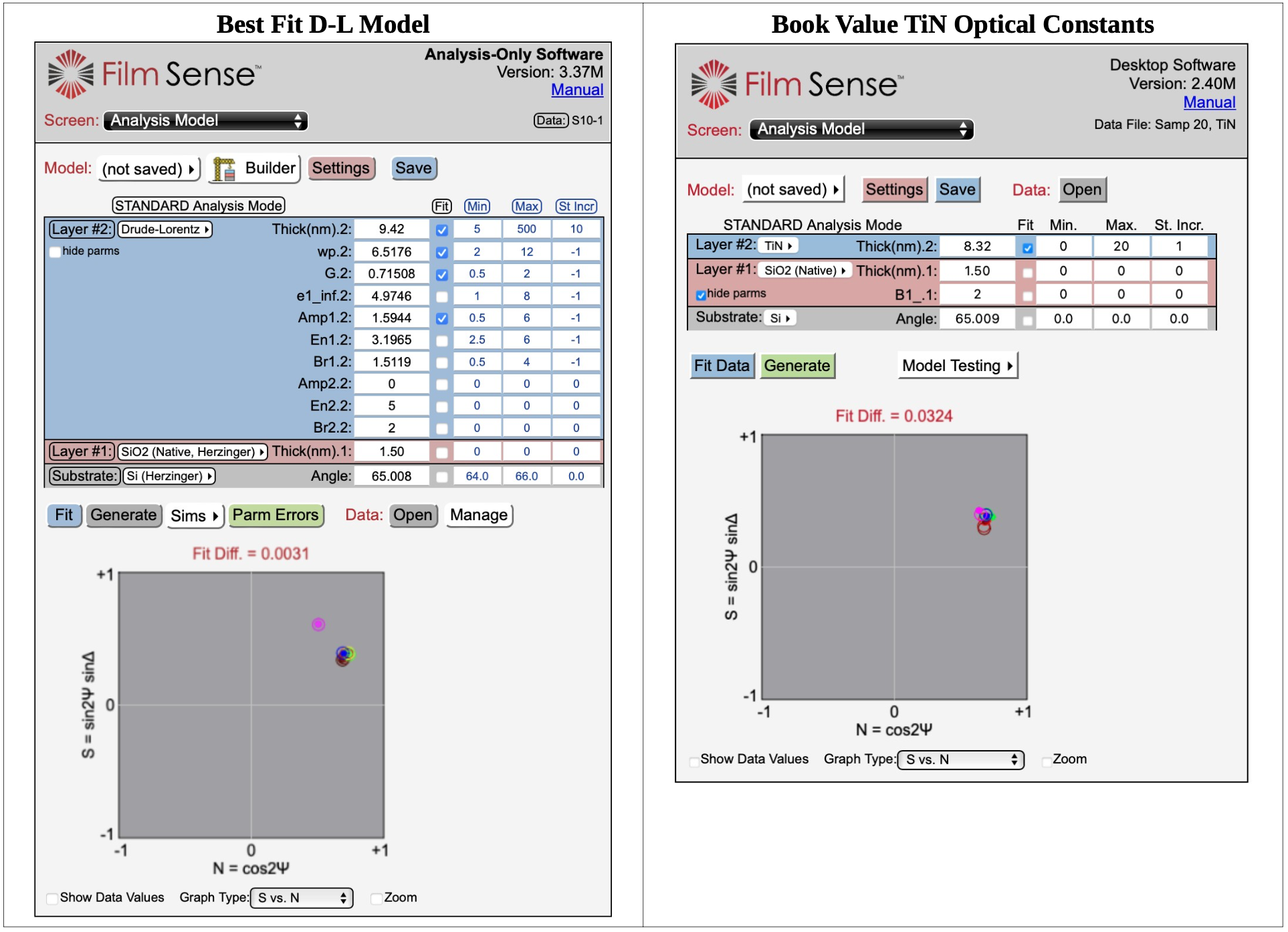
Sample #10: 10 nm TiN on Si
Titanium nitride (TiN) is a metallic material, and its optical properties are strongly dependent on the deposition conditions (this film was deposited by ALD). Book value optical constants provided a poor fit (model below right); the Best Fit model (below left) used a Drude-Lorentz dispersion layer. A Drude-Lorentz (D-L) dispersion equation is commonly used to represent the TiN dielectric function (E. Langereis, et. al., J. Appl. Phys. 100, p. 023534, 2006). The Drude terms (wp: plasma frequency, and G: damping factor, which can be used to calculate the film resistivity) account for the free electron absorption (which is strongly depending on the grain size and film thickness), while the Lorentz oscillator(s) account for the interband absorptions in the TiN. (Some of the D-L parameters were fixed at values determined from a multi-sample analysis.) This sample demonstrates that D-L oscillator parameters and film resistivity can be determined with good precision and accuracy with the FS-8 multi-wavelength ellipsometric data set (spectroscopic data is not required).
Transparent Film (Si3N4): Measuring Thickness and Index of Refraction
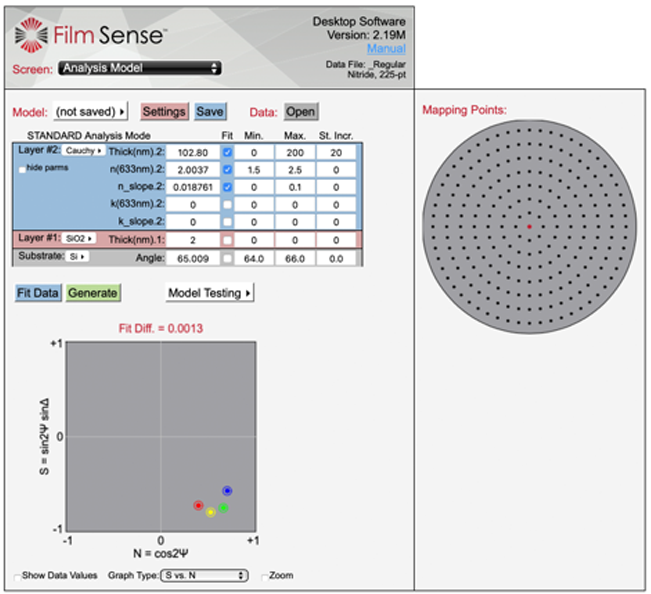
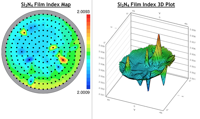
In the example below, the film thickness and refractive index uniformity was measured by a Film Sense FS-XY150 automated mapping system. The optical model used for the data analysis included a 2 nm native oxide film on the Si wafer substrate, and a “Cauchy” layer to represent the transparent Si3N4 film.
Si3N4 on Si Optical Model
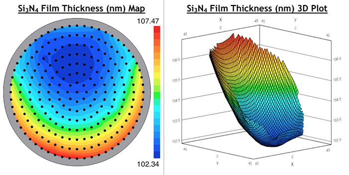
The mapping results are shown in the contour and 3D plots below. The thickness variation for the nominal 100 nm film is approximately 5 nm. Note that the 3D plot was rotated to provide the best view of the thickness non-uniformity.
The index of refraction is very uniform across the wafer, with a peak to peak variation less than 0.01. The index variation is even lower if the high and low points are removed from the map.
Film Sense – Thin Film Measurement
Multilayer Oxide-Nitride-Oxide (ONO) Sample: Measuring Multiple Layer Thicknesses
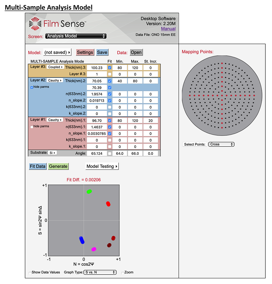
In this example, multiple film thicknesses were determined by a Film Sense FS-RT300 automated mapping system. When measuring a multilayer sample, it is preferable to determine the optical constants of the constituent layers by measuring single layer films. However, this is not always possible, as was the case for this example. Multi-Sample analysis is a powerful method for increasing the information content in the analysis, which in turn can provide more accurate layer optical constants. In the model below, multiple data points were selected from the mapping scan (in a “cross” pattern), and were simultaneously analyzed to determine the 3 layer thicknesses, and the index of refraction of the oxide and nitride layers (the optical constants of the top and bottom oxide were coupled together). The thickness variation across the wafer is actually beneficial for this analysis, as the different measurement points act as multiple “samples” with different layer thicknesses. The index of refraction values which were determined in the multi-sample analysis were then fixed, and the 3 layer thicknesses were fit when re-analyzing the full mapping data set.
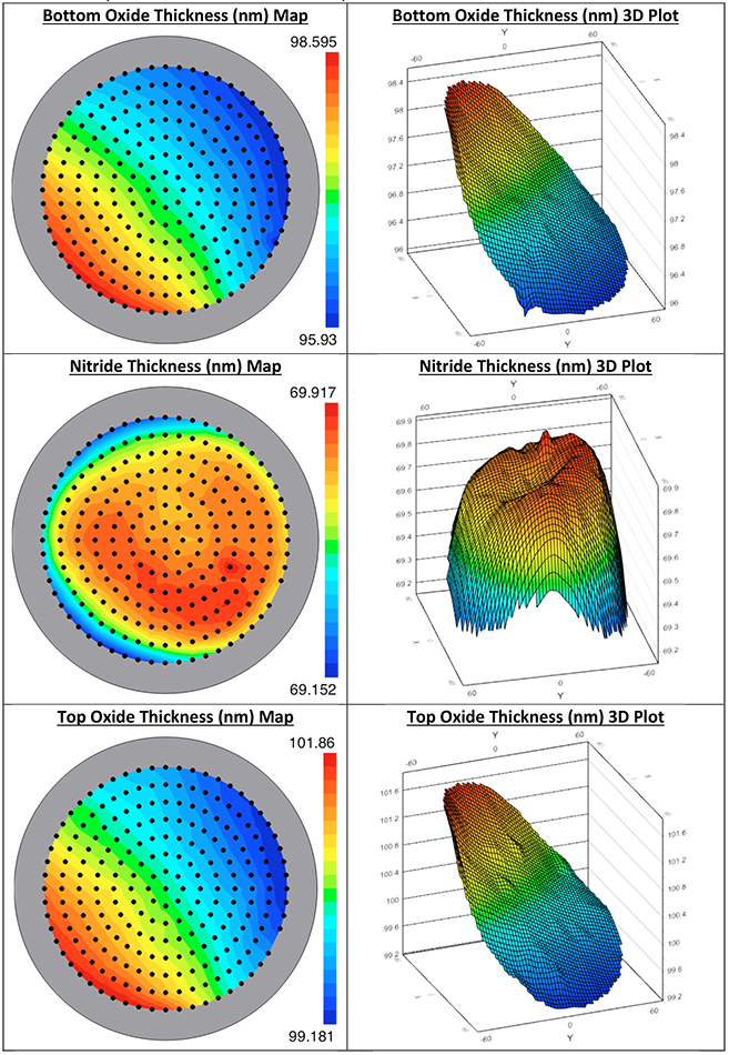
The mapping results of the 3 layer thicknesses are shown in the contour and 3D plots below. Note that the top and bottom oxide layers exhibit similar thickness non-uniformity patterns, which are very different the middle nitride layer.
100 nm of HfO2
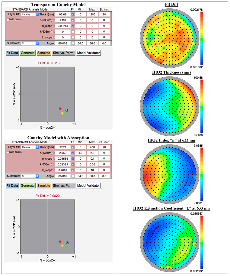
HfO2 Wafer: The initial model fit, which assumed a transparent Cauchy layer, resulted in a somewhat high Fit Diff value of 0.0116. Allowing absorption in the film (by fitting for the “k” terms in the Cauchy layer) significantly reduced the Fit Diff to 0.002. The wafer maps show that the film n & k values are relatively constant, while the thickness varies ≈ 5 nm.
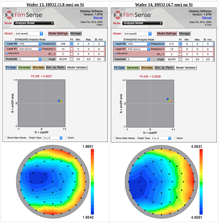
Wafers 13 and 14, HfO2 (1.8 and 4.7 nm) on Si: Book value HfO2 optical constants were used in the optical models below, along with an assumed native oxide thickness of 1.5 nm. The model fits (for data at the wafer center) and thickness uniformity maps are shown below. The FS-1 determined thicknesses are in good agreement with the nominal values.
Thin Transparent Films on Si
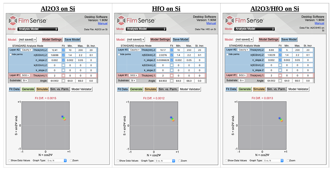
- The built in “Cauchy on Si” model was used as a starting point for the data analysis, but with the following modifications:
- A native oxide layer was added to the optical model (with an assumed thickness of 2 nm)
- The “Min.” film thickness was reduced to 5 nm, and the “Max.” index was increased to 2.2, as some of the films exceed the ranges of the parameter bounds in the standard “Cauchy on Si” model.
- The resulting data fits and Fit Diff values are all very good, and the index values are typical for Al2O3 and HfO2 films.
