Automated Mapping Systems
Fast, accurate, and reliable thin film thickness uniformity measurements
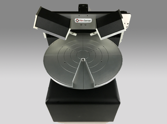
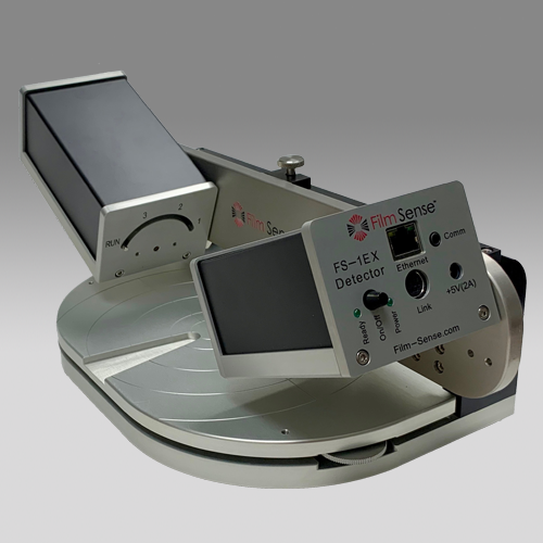
The FS-RT300 combines an FS-8 Multi-Wavelength Ellipsometer with a compact automated mapping stage to provide fast, accurate, and reliable film thickness uniformity measurements across a wafer.
Features and Specifications
-
8 wavelengths of ellipsometric data (370, 450, 525, 595, 660, 735, 850, 950 nm), with long life LED sources, and no moving parts detector
-
Accurate thickness measurements for most transparent thin films from 0 – 5 μm
-
Typical time for wafer map: 2.5 minutes (49 points on a 300 mm diameter wafer)
-
Typical thickness repeatability: 0.002 nm
-
Integrated focusing probes, standard spot size: 0.8 x 1.9 mm (other spot sizes available)
-
Compact footprint: 400×500 mm, 22 kg
-
Stage travel: R (linear) 150 mm, resolution: 12 μm, Theta (rotation) 360°, resolution: 0.05°
-
USB camera option available
-
Motorized Z-stage for sample auto alignment
-
Contour and 3D plots of measured parameters
-
Flexible Scan Pattern Editor
FS-RT300
AUTOMATED MAPPING
Thin Film Thickness Uniformity Measurement Examples
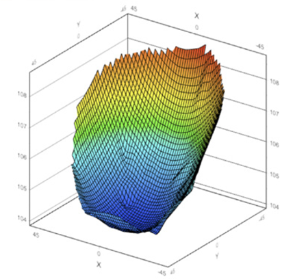
Example of 3-D Plot for Film Sense mapping systems for thin film thickness measurements
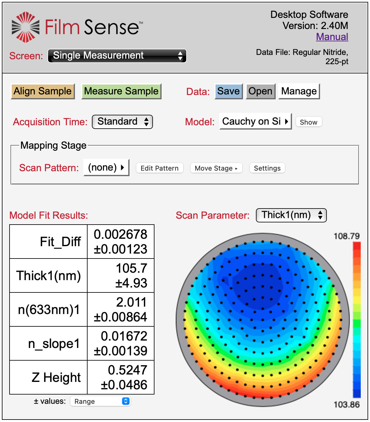
Software screen for operating Film Sense mapping systems, and displaying the measurement results
Send Us Your Samples
As thin film applications are so varied and diverse, the best way to determine if a Film Sense Multi-Wavelength Ellipsometer is right for your application is to perform demonstration measurements on your actual samples. Please contact us to discuss your application, and arrange for sample measurements.
Testimonial
“We have purchased four Film Sense products for our small R&D group. We have three FS-1 units and one FS-1EX unit with the RT300 mapping stage. The Film Sense software is the most intuitive and easiest to use of all the ellipsometers I have experience using. Our favorite feature is the multi-sample analysis method. This feature allows you to determine the optical constants for new or poorly fitting films by simply measuring a small number of samples with various thicknesses. Having knowledge of the actual thin film thickness values is not even necessary. The software understands the optical constants must be the same for all samples, and each sample varies only in thin film thickness. The user just needs to collect the data and press the fit button. New films layers are created in just a couple of minutes. We also love the automatic adjustment for sample height on the RT300 mapping stage. Our process engineers are constantly adjusting the height on competitor’s units without this automatic feature.”
-Staff Systems Engineer at large semiconductor OEM
“The system is great and we are having an increase of users using it. I am happy with the system and I direct users to use it when I am training them on our ALD deposition system. It gives great results and the customer support is quick and helpful too.”
– Tony Whipple, Scientist
Minnesota Nano Center
Transparent Film (Si3N4): Measuring Thickness and Index of Refraction
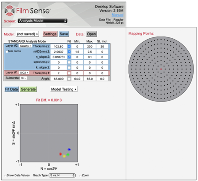
In the example below, the film thickness and refractive index uniformity was measured by a Film Sense FS-XY150 automated mapping system. The optical model used for the data analysis included a 2 nm native oxide film on the Si wafer substrate, and a “Cauchy” layer to represent the transparent Si3N4 film.
Si3N4 on Si Optical Model
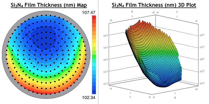
The mapping results are shown in the contour and 3D plots below. The thickness variation for the nominal 100 nm film is approximately 5 nm. Note that the 3D plot was rotated to provide the best view of the thickness non-uniformity.
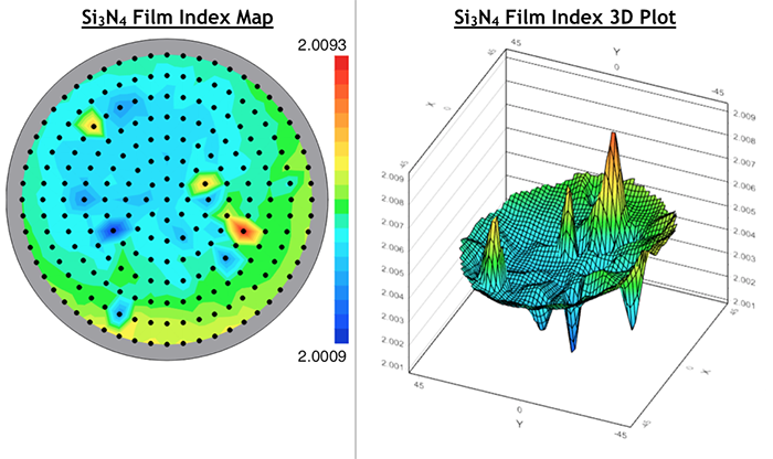
The index of refraction is very uniform across the wafer, with a peak to peak variation less than 0.01. The index variation is even lower if the high and low points are removed from the map.
Film Sense – Thin Film Thickness
Multilayer Oxide-Nitride-Oxide (ONO) Sample: Measuring Multiple Layer Thicknesses
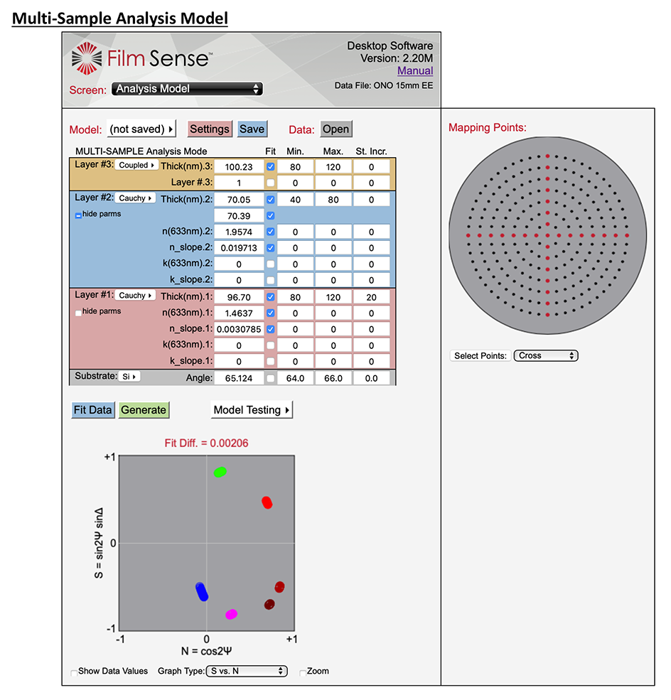
In this example, multiple film thicknesses were determined by a Film Sense FS-RT300 automated mapping system. When measuring a multilayer sample, it is preferable to determine the optical constants of the constituent layers by measuring single layer films. However, this is not always possible, as was the case for this example. Multi-Sample analysis is a powerful method for increasing the information content in the analysis, which in turn can provide more accurate layer optical constants. In the model below, multiple data points were selected from the mapping scan (in a “cross” pattern), and were simultaneously analyzed to determine the 3 layer thicknesses, and the index of refraction of the oxide and nitride layers (the optical constants of the top and bottom oxide were coupled together). The thickness variation across the wafer is actually beneficial for this analysis, as the different measurement points act as multiple “samples” with different layer thicknesses. The index of refraction values which were determined in the multi-sample analysis were then fixed, and the 3 layer thicknesses were fit when re-analyzing the full mapping data set.
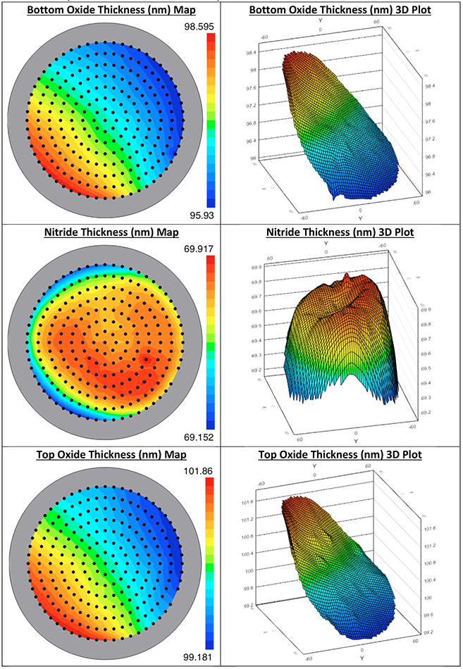
The mapping results of the 3 layer thicknesses are shown in the contour and 3D plots below. Note that the top and bottom oxide layers exhibit similar thickness non-uniformity patterns, which are very different the middle nitride layer.
Film Sense – Thin Film Thickness
100 nm of HfO2
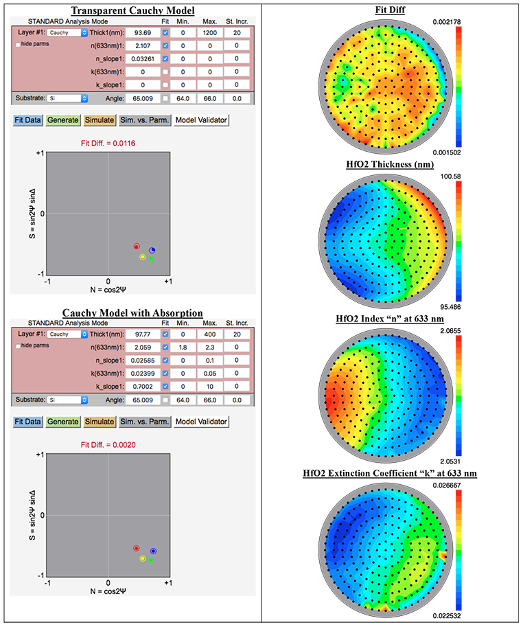
HfO2 Wafer: The initial model fit, which assumed a transparent Cauchy layer, resulted in a somewhat high Fit Diff value of 0.0116. Allowing absorption in the film (by fitting for the “k” terms in the Cauchy layer) significantly reduced the Fit Diff to 0.002. The wafer maps show that the film n & k values are relatively constant, while the thickness varies ≈ 5 nm.
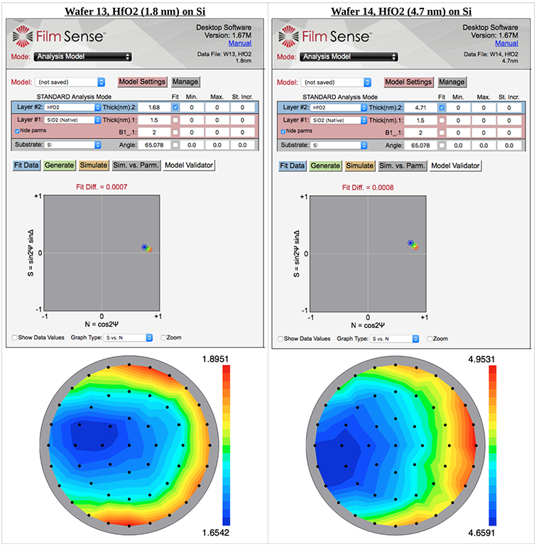
Wafers 13 and 14, HfO2 (1.8 and 4.7 nm) on Si: Book value HfO2 optical constants were used in the optical models below, along with an assumed native oxide thickness of 1.5 nm. The model fits (for data at the wafer center) and thickness uniformity maps are shown below. The FS-1 determined thicknesses are in good agreement with the nominal values.
Thin Transparent Films on Si
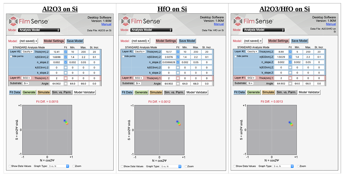
- The built in “Cauchy on Si” model was used as a starting point for the data analysis, but with the following modifications:
- A native oxide layer was added to the optical model (with an assumed thickness of 2 nm)
- The “Min.” film thickness was reduced to 5 nm, and the “Max.” index was increased to 2.2, as some of the films exceed the ranges of the parameter bounds in the standard “Cauchy on Si” model.
- The resulting data fits and Fit Diff values are all very good, and the index values are typical for Al2O3 and HfO2 films.
